Mastering High-Reliability Aerospace Electronics: A Comprehensive Guide from Design to Production
This guide provides an end-to-end blueprint for developing and manufacturing high-reliability electronics for the aerospace sector, navigating complexities from initial design through to final production. In essence, it is a definitive manual for mission-critical success.
1. The Unique Demands of Aerospace Electronics
Electronics in aerospace applications face challenges far exceeding commercial standards. This environment demands a fundamentally different approach to design and manufacturing, where failure is not an option. Here, reliability is engineered, not assumed.

Surviving Extreme Mission Environments
Aerospace systems must function from extreme heat near engines to the cryogenic cold of space. These thermal swings cause mechanical stress on all components, solder joints, and substrates, demanding robust material selection and meticulous thermal analysis. Thermal resilience is non-negotiable.
Pressure and altitude variations present unique dangers, including material outgassing that can contaminate optics. The vacuum of space also lowers dielectric strength, increasing risks of electrical arcing in high-voltage circuits. Careful material and layout choices are crucial for performance.
Intense vibration from engines, coupled with severe shocks during launch and landing, compromises mechanical integrity. Components require secure anchoring, and connectors need robust locking features to prevent intermittent failures. In short, mechanical stability is paramount for mission survival.
Proactively Anticipating Common Failure Modes
Solder joint fatigue is a primary concern, often induced by mismatched coefficients of thermal expansion (CTE) between components and the PCB. This stress is a leading cause of intermittent and hard failures over the product’s lifecycle. Mitigating CTE mismatch is a core design goal.
Moisture ingress can lead to corrosion and short circuits, while connector fretting from micro-vibrations can degrade signal integrity. Unwanted electromagnetic interference (EMI) can disrupt sensitive circuits, requiring careful shielding. Protecting against these factors is essential.
Conformal coatings and potting compounds, while protective, can introduce their own failure modes. They can create mechanical stress during thermal cycling or trap moisture if applied incorrectly, leading to latent defects. Thus, their application requires precise process control.
Foundational Design Responses for Mission Success
A strict component derating policy is fundamental. Operating components well below their specified maximum ratings for voltage, current, and temperature dramatically increases their lifespan and reliability. Derating provides a crucial safety margin against unforeseen stress.
Redundancy and fail-safe mechanisms are critical for systems where a single point of failure could be catastrophic. This involves duplicating critical circuits or implementing designs that default to a safe state if a fault occurs. This design philosophy ensures operational continuity.
High-voltage circuits demand strategic creepage and clearance distances on the PCB to prevent arcing. Robust grounding, shielding, and isolation schemes are equally vital to ensure signal integrity and electromagnetic compatibility (EMC). These rules are foundational for electrical safety and performance.
FAQs
Q: Why is thermal management so critical?
A: Extreme temperature swings cause mechanical stress, leading to material and solder joint failures.
Q: What is component derating?
A: It's the practice of using components far below their max ratings to boost reliability and lifespan.
2. Navigating the Aerospace Standards & Compliance Maze
Adherence to a rigorous set of standards is mandatory in the aerospace industry. These frameworks govern every aspect of design, manufacturing, and quality, ensuring safety and interoperability across the supply chain. Compliance is the bedrock of aerospace quality.
Essential Quality & Process Frameworks
AS9100 is the cornerstone quality management system (QMS) for the aerospace industry. It builds upon ISO 9001, adding specific requirements for quality, safety, and reliability that are unique to this demanding sector. Certification to AS9100 is a key indicator of a supplier's capability.
AS9145, or Advanced Product Quality Planning (APQP), provides a structured process for new product development. It is complemented by AS9102 for First Article Inspection (FAI), ensuring that the production process can reliably produce conforming parts. These standards formalize product realization.
A disciplined change control process is vital for maintaining product integrity after qualification. Any modification must be rigorously evaluated, documented, and approved. The Material Review Board (MRB) is responsible for dispositioning non-conforming material. This ensures strict process discipline.
Mandates for Workmanship, Materials & Handling
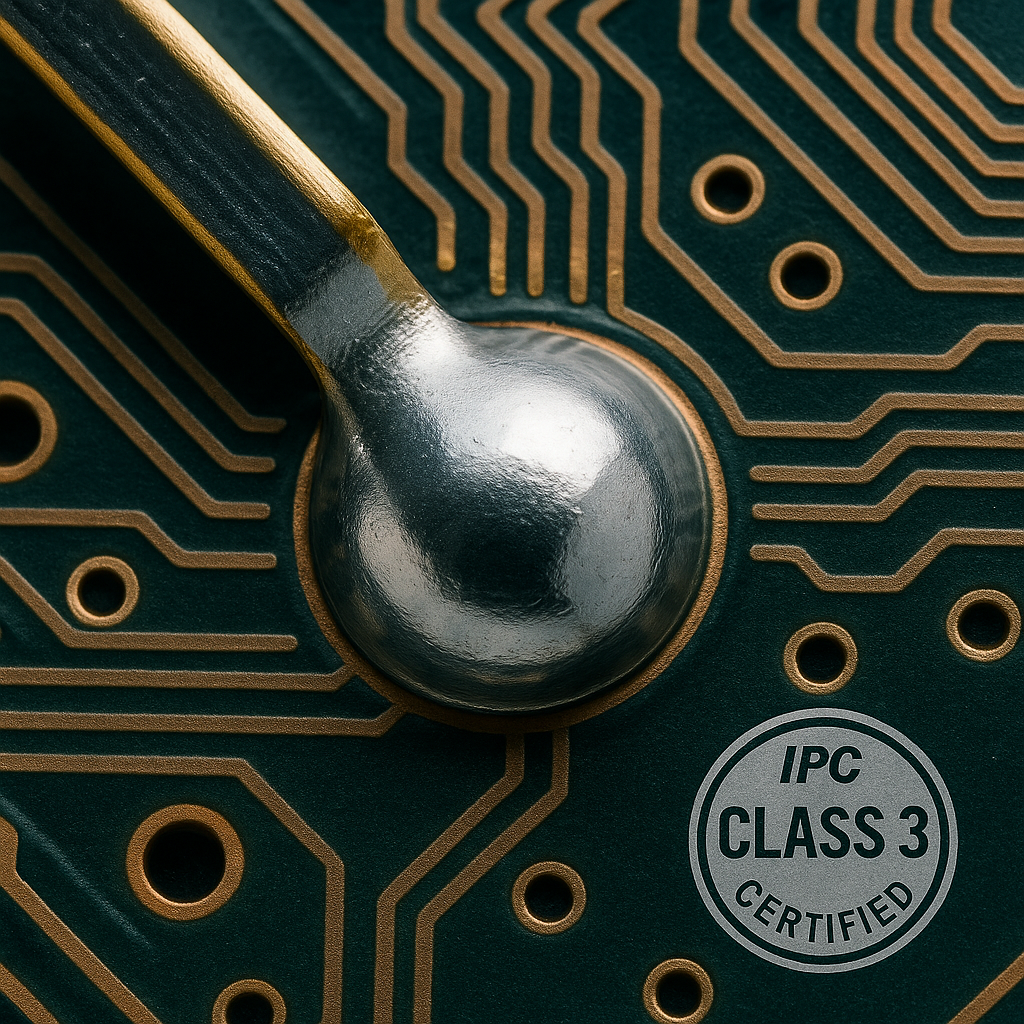
IPC-A-610 Class 3 and J-STD-001 Class 3 define the highest level of workmanship for electronic assemblies. These standards set acceptance criteria for everything from solder joints to component mounting for high-performance products. Class 3 is the default for mission-critical aerospace hardware.
IPC-6012DS specifies requirements for rigid printed circuit boards intended for space and military avionics. It addresses specific reliability concerns for these applications that go beyond standard commercial PCB fabrication. This standard ensures the bare board is fit for purpose.
Electrostatic discharge (ESD) can destroy sensitive electronic components with an invisible spark. The ESD S20.20 standard outlines the requirements for establishing, implementing, and maintaining an effective ESD control program. This protects hardware throughout the manufacturing lifecycle.
Environmental & Electromagnetic Compatibility Regulations
DO-160 (for commercial aviation) and MIL-STD-810 (for military) are the definitive standards for environmental testing. They specify a range of tests, from vibration and shock to humidity and fungus resistance, to prove a product's survivability. Passing these tests is mandatory for qualification.
Regulations like RoHS (Restriction of Hazardous Substances) and REACH (Registration, Evaluation, Authorisation and Restriction of Chemicals) govern material content. Full material declarations are often required to prove compliance. This ensures environmental responsibility and market access.
FAQs
Q: What is the most important quality standard in aerospace?
A: AS9100 is the foundational quality management system standard for the entire aerospace industry.
Q: Why is IPC Class 3 workmanship required?
A: It ensures the highest level of assembly quality and reliability needed for mission-critical systems.
3. Advanced Materials & PCB Stack-Up Engineering
The physical foundation of a reliable electronic assembly is its printed circuit board (PCB). Material selection and stack-up design are not trivial choices; they are critical engineering decisions that dictate performance and reliability. Smart material choices form the product's backbone.
Laminate Selection: Beyond Standard FR-4
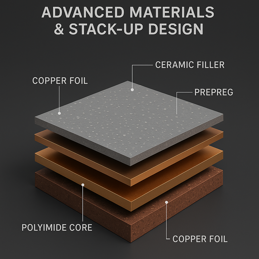
While standard FR-4 is common, aerospace applications often require laminates with a higher glass transition temperature (Tg) to withstand extreme operational heat. High-Tg FR-4, Polyimide, and ceramic-filled materials offer superior thermal performance. The right laminate prevents delamination and failure.
For high-frequency RF and microwave circuits, specialized materials like PTFE-based or hybrid laminates are necessary. Their controlled dielectric constant (Dk) and low dissipation factor (Df) are essential for maintaining signal integrity and minimizing loss. Material choice dictates RF performance.
Copper & Via Strategy for High-Density Designs
Copper weight, or thickness, must be carefully planned to manage both current-carrying capacity and thermal dissipation. Heavier copper can help spread heat from powerful components but introduces manufacturing challenges. This balancing act is crucial for power and thermal integrity.
As designs become denser, microvias and stacked vias are used to connect layers. However, these structures introduce their own reliability concerns, particularly regarding their susceptibility to cracking under thermal stress. Their reliability must be rigorously verified.
Via-in-pad technology, where vias are placed directly on BGA pads and filled with conductive or non-conductive resin, is key for high-density routing. This technique improves routing density but requires precise manufacturing control to ensure a flat, solderable surface. It enables next-gen device support.
Designing Effective Thermal Management Paths
Thermal vias are arrays of plated through-holes placed under a hot component to conduct heat to other layers or a heatsink. When combined with integrated heat spreaders, they create an effective path for thermal energy to escape. This prevents components from overheating. [Jump to H2: Managing Cost, Schedule & Risk]
Thermal Interface Materials (TIMs) are applied between a component and its heatsink to fill microscopic air gaps and improve heat transfer. A clear policy defining the type, thickness, and application method of TIMs is essential for consistent thermal performance. TIMs are a critical thermal link.
Bottom-Terminated Components (BTCs) like QFNs can easily trap heat if not designed for properly. A dense pattern of thermal vias in the central ground pad is non-negotiable for pulling heat away from the die. Proper BTC layout prevents localized hotspots.
Surface Finish Selection & Associated Risks
The choice of PCB surface finish impacts solderability, reliability, and cost. Electroless Nickel Immersion Gold (ENIG) is popular but carries the risk of "black pad." ENEPIG, Immersion Silver, and Immersion Tin are alternatives with different trade-offs. Each finish has unique process considerations.
Risks associated with finishes include tin whiskers, which can grow from pure tin and cause short circuits, and gold embrittlement in solder joints with excessive gold thickness. Understanding and mitigating these risks is vital for long-term reliability. A flawed finish can doom a product.
FAQs
Q: Why not always use standard FR-4 laminate?
A: Aerospace needs materials with higher temperature resistance and better RF performance than FR-4.
Q: What is the purpose of a thermal via?
A: It acts like a heat pipe, conducting thermal energy away from a hot component to cooler PCB layers.
4. Implementing a Robust Design for Excellence (DFX) Framework
A successful aerospace product is not just functional; it is manufacturable, testable, and reliable. The Design for Excellence (DFX) framework embeds these considerations into the design process from the very beginning. DFX is proactive engineering for lifecycle success.
Design for Manufacturing (DFM): Ensuring Producibility
DFM rules ensure a design can be physically built with high yield. This includes defining minimum trace widths, spacing, via aspect ratios, and annular ring sizes that align with the chosen fabricator's capabilities. Adhering to DFM rules prevents costly manufacturing failures.
Best practices for complex assemblies include specifying generous bend radii for rigid-flex circuits to prevent stress cracking. It is also critical to define component keep-outs to allow clearance for automated coating or potting processes. These rules ensure mechanical and process compatibility.
Design for Test (DFT): Building in Verifiability
DFT involves designing the product to be easily and thoroughly testable. This means setting clear targets for test coverage for methods like In-Circuit Test (ICT) and Functional Circuit Test (FCT). High test coverage is essential for catching manufacturing defects early. [Jump to H2: Proving Performance]
For complex digital circuits, ensuring boundary scan chain integrity is a key DFT principle. This allows for testing connections between large integrated circuits without physical probing. Providing accessible ports for on-board programming is also crucial. DFT enables comprehensive verification.
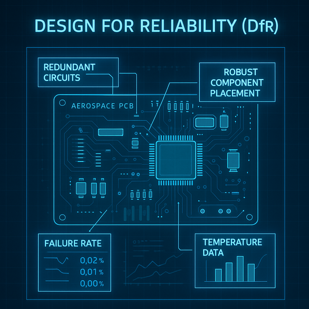
Design for Reliability (DFR): Engineering for Longevity
DFR focuses on ensuring the product survives its intended mission life. A core tenet is enforcing strict component derating rules to minimize stress on parts. This single practice has a profound impact on long-term reliability. Derating is the foundation of robust hardware design.
Connectors are a common point of failure, so DFR specifies robust retention and locking mechanisms to withstand vibration. A clear plan for conformal coating masking is also critical to protect connectors and test points. These details prevent common field failures.
While potting provides rugged protection, it can make rework impossible. A DFR strategy includes developing a clear policy on which areas may be potted and establishing procedures for rework where feasible. This balances protection with serviceability requirements.
FAQs
Q: What is DFX?
A: Design for Excellence. It's a philosophy of designing for manufacturing, testing, and reliability.
Q: Why is DFT important?
A: It builds testability into the design, enabling high-coverage testing to catch defects early.
5. Critical Control Points in the Manufacturing Flow
Transitioning a design to production requires rigorous process control. Identifying and monitoring Critical Control Points (CCPs) in the manufacturing flow is essential to ensure that design intent is translated into a reliable product. Process control is where design meets reality.

The Gated NPI Process: From DFM to Production
The New Product Introduction (NPI) process should be managed with formal gates. Key gates include DFM review, tooling release, First Article Inspection (FAI), pilot production runs, and final qualification or PPAP. A gated process ensures disciplined, sequential progress.
Once a product is qualified, any change to the design, materials, or process must be managed through a disciplined change control board. Uncontrolled changes are a primary cause of quality escapes in mature production. This rigor maintains the qualified state of the product.
Identifying & Monitoring Critical Control Points (CCPs)
Solder Paste Inspection (SPI) is a crucial CCP. It verifies the volume and alignment of solder paste deposits before component placement, preventing many common soldering defects. Proper reflow oven profiling is another, ensuring all parts reach the correct temperature. These CCPs control solder joint quality.
For assemblies with BGAs and BTCs, automated X-ray inspection (AXI) is a critical step. It allows for non-destructive inspection of hidden solder joints, checking for voids, shorts, and opens. Clear accept/reject criteria for X-ray images are essential. AXI is vital for complex component inspection.
Processes like conformal coating and potting are CCPs. Thickness and adhesion of coatings must be tightly controlled. Ionic cleanliness testing before coating ensures no contaminants are sealed in, preventing future corrosion. Controlling these final steps is key to long-term reliability.
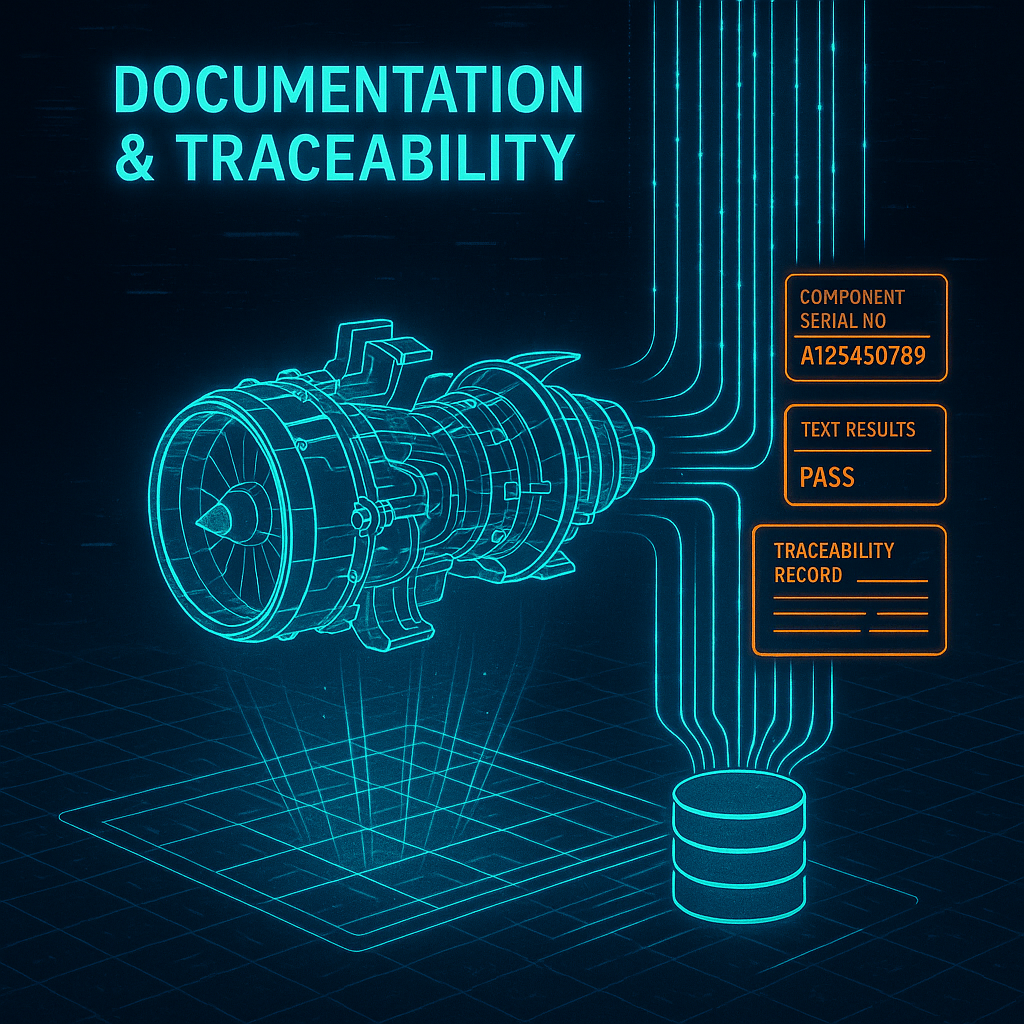
The Role of End-to-End Digital Traceability
Board-level serialization, often using a 2D matrix code, is the foundation of digital traceability. Every single board is given a unique identity, allowing its journey to be tracked throughout the entire manufacturing process. Serialization enables granular data collection.
A Manufacturing Execution System (MES) should be used to capture data at each step. This includes linking the board's serial number to the specific materials used, operators, machine parameters, and timestamps. This digital thread provides unprecedented process insight. [Jump to H2: Assembling the Essential Documentation Pack]
Manufacturing Critical Control Point Examples
| Control Point | Purpose | Key Metrics | Compliance Standard |
|---|---|---|---|
| Solder Paste Inspection (SPI) | Prevent solder defects before reflow | Volume, Area, Height, Offset | IPC-7527 |
| Automated X-Ray (BGA/BTC) | Inspect hidden solder joints | Void Percentage, Bridge Detection | IPC-7095 |
| Conformal Coat Thickness | Ensure adequate environmental protection | Thickness (microns), Coverage | IPC-CC-830 |
| Ionic Cleanliness Test | Verify board is free of corrosive flux residues | µg NaCl eq./cm² | IPC-J-STD-001 |
FAQs
Q: What is a "gated" NPI process?
A: It's a structured launch process with formal reviews and approvals required at each key stage.
Q: Why is digital traceability important?
A: It allows for precise root cause analysis if a defect is found, tracing it back to a specific batch or process.
6. Proving Performance: Qualification & Reliability Testing
Design and process controls are theoretical until proven. A rigorous regime of qualification and reliability testing provides the empirical evidence that a product meets all performance and reliability requirements. Testing is the ultimate arbiter of product quality.

Comprehensive Electrical Verification
In-Circuit Test (ICT), Flying Probe, and Functional Circuit Test (FCT) provide electrical verification of the assembly. The goal is to maximize test coverage to catch component and manufacturing defects. Measuring this coverage is a key metric for test effectiveness.
High Potential (HiPot) testing verifies the insulation integrity between high-voltage circuits, ensuring there is no risk of dielectric breakdown. Surface Insulation Resistance (SIR) testing checks for contaminants that could cause current leakage. These tests ensure electrical safety.
Rigorous Environmental Stress Screening (ESS)
ESS involves subjecting the product to stresses beyond its normal operating range to precipitate latent defects. This includes thermal cycling, random vibration, and shock testing according to standards like DO-160 and MIL-STD-810. ESS proves the product's ruggedness.
Highly Accelerated Life Testing (HALT) and Highly Accelerated Stress Screening (HASS) are aggressive test-to-fail methods. They are used during development to quickly find the weakest links in a design. HALT/HASS helps establish the true operational limits of the product.
Defining Acceptance Criteria & Process Metrics
Clear, objective pass/fail criteria must be defined for every test. For production, statistical sampling plans (e.g., AQL) determine how many units from a batch must be tested to ensure overall quality. This data-driven approach ensures consistent quality control.
Key process metrics like First Time Yield (FTY) and Defects Per Million Opportunities (DPMO) are used to monitor the health of the manufacturing process. These metrics provide a baseline for continuous improvement activities. They are the vital signs of a manufacturing line.
FAQs
Q: What is the purpose of Environmental Stress Screening (ESS)?
A: To force hidden (latent) defects to appear by exposing the product to harsh, controlled stress.
7. A Toolkit for Supplier Selection & Auditing
The quality of your product is inextricably linked to the capability of your manufacturing partners. A systematic and objective process for selecting, auditing, and managing suppliers is not just good practice; it is a critical risk mitigation strategy. A strong supply chain is a competitive advantage.

Assessing Supplier Technical Capabilities
A supplier must have proven experience with the specific technologies your design requires, such as rigid-flex PCBs, controlled impedance, or via-in-pad. Ask for evidence of past projects and verify their technical claims. This ensures their capabilities match your needs.
Evaluate the extent of their in-house capabilities. A supplier that can perform special processes like conformal coating, potting, and advanced X-ray inspection internally has better control over quality and lead times. In-house capability reduces supply chain complexity.
Evaluating Quality Systems & Risk Management
AS9100 certification is a primary requirement for an aerospace supplier. If not certified, they should have a clear and credible roadmap to achieve it. An audit should also confirm robust ESD S20.20 discipline on the manufacturing floor. This demonstrates a commitment to quality.
The supplier must have a documented counterfeit component mitigation plan, compliant with AS5553. They also need processes for managing component obsolescence and ensuring compliance with export control regulations like ITAR/EAR. These plans are crucial for risk management.
Using a Weighted Scorecard for Objective Evaluation
A weighted scorecard is a powerful tool for comparing potential suppliers objectively. It allows you to score each supplier across key criteria like technical skill, quality systems, delivery performance, and cost. This data-driven approach removes bias from the selection process.
Within the scorecard, establish non-negotiable "go/no-go" thresholds for critical items like AS9100 certification or a counterfeit parts plan. This ensures that any supplier you consider meets your minimum requirements for partnership. It defines your baseline for quality.
FAQs
Q: What is the most important factor when selecting a supplier?
A: A certified AS9100 quality system and proven technical capability in your required technologies.
8. Assembling the Essential Documentation Pack for Build
A flawless transition from design to manufacturing depends on a complete and unambiguous documentation package. This "tech data pack" is the contract between the design team and the manufacturing floor. Clarity and completeness in documentation prevent costly errors.
Core Design Data Requirements
Modern manufacturing data formats like ODB++ or IPC-2581 are preferred over traditional Gerber files. They package all necessary layer, drill, and netlist information into a single intelligent file, reducing the risk of data misinterpretation. These formats build-in design intelligence.
The package must include a detailed stack-up report specifying all materials, thicknesses, and dielectric properties. An impedance specification list is also critical for high-speed designs. These documents define the PCB's physical and electrical DNA.
Comprehensive fabrication and assembly drawings are still essential. They communicate critical information that data files alone cannot, such as dimensions, tolerances, special instructions, and final quality requirements. The drawings serve as the ultimate reference.
Critical Specifications & Control Lists
The Bill of Materials (BOM) must be precise, listing not just part numbers but also an Approved Vendor List (AVL) for each component. This helps control the supply chain and prevent the use of unauthorized parts. A well-managed BOM is a cornerstone of supply chain integrity.
Detailed test specifications, firmware versions, and acceptance criteria must be clearly documented. Any ambiguity here will lead to disputes and delays. For special processes, detailed work instructions for coating and potting are mandatory. Clear instructions ensure process consistency.
Required Process Control Documentation
A master Control Plan should be created, which summarizes all the critical process control points, from incoming inspection to final test. This document provides a high-level map of the entire quality assurance strategy. The Control Plan is the blueprint for manufacturing quality.
The data pack should also include the supplier's specific ESD control plan and their procedures for handling moisture-sensitive components (MSL). This confirms that they have the necessary controls in place to protect the hardware during assembly. It verifies their process readiness.
FAQs
Q: Why is ODB++ better than Gerber files?
A: ODB++ is an intelligent format that bundles all design data, reducing errors and ambiguity.
9. Managing Cost, Schedule & Risk
Beyond the technical challenges, aerospace electronics projects require disciplined project management. Effectively managing cost drivers, creating realistic schedules, and proactively mitigating risks are essential for commercial success. Project management ensures on-time, on-budget delivery.

Identifying Key Cost Drivers
PCB cost is driven by factors like layer count, via technology (e.g., microvias), and the choice of advanced materials and surface finish. Similarly, the required test coverage directly impacts cost. Understanding these drivers allows for informed design trade-offs. This is key to cost optimization.
Realistic Scheduling & Lead Time Management
Project schedules must be built with realistic timelines for each phase: design, tooling, fabrication, FAI, and qualification. Overly optimistic schedules are a common cause of project failure. A realistic schedule accounts for the complexities of each stage.
Long-lead-time components and specialized PCB laminates are a major scheduling risk. These items should be identified and ordered early in the project. Building buffer time into the schedule for these critical path items is prudent risk management. Proactive procurement is essential.
Proactive Risk Management
A formal risk register should be created and maintained throughout the project. It should document potential risks related to part supply, single-source components, technical challenges, and requalification triggers. Each risk needs a clear owner and a mitigation plan.
By assigning clear ownership for each identified risk, you ensure accountability for developing and executing mitigation actions. The risk register should be a living document, reviewed regularly by the project team. This structured approach turns risk management from a reactive to a proactive discipline.
FAQs
Q: What is a major cost driver in a PCB?
A: Advanced technologies like high layer counts, microvias, and specialized high-frequency materials.
10. Lessons from the Field: Real-World Case Studies
Theoretical knowledge finds its true value in practical application. These real-world case studies illustrate how the principles discussed in this guide are used to diagnose and solve complex engineering challenges. These examples demonstrate the principles in action.
For more insights and technical discussions, please feel free to [Visit My LinkedIn Article for More Details].
Case Study 1: Solving Vibration Failure in an Avionics RF Module
An RF module was experiencing intermittent failures during vibration testing. Analysis revealed that a large BGA component was flexing, causing micro-cracks in the solder balls. The root cause was excessive board flex under the component. This analysis pinpointed the mechanical failure mode.
The solution involved a two-part redesign. Via-in-pad with non-conductive epoxy fill was used to strengthen the area under the BGA. Additionally, a strategically placed board stiffener was added to the PCB to reduce overall flex. The redesigned module passed vibration testing with margin.
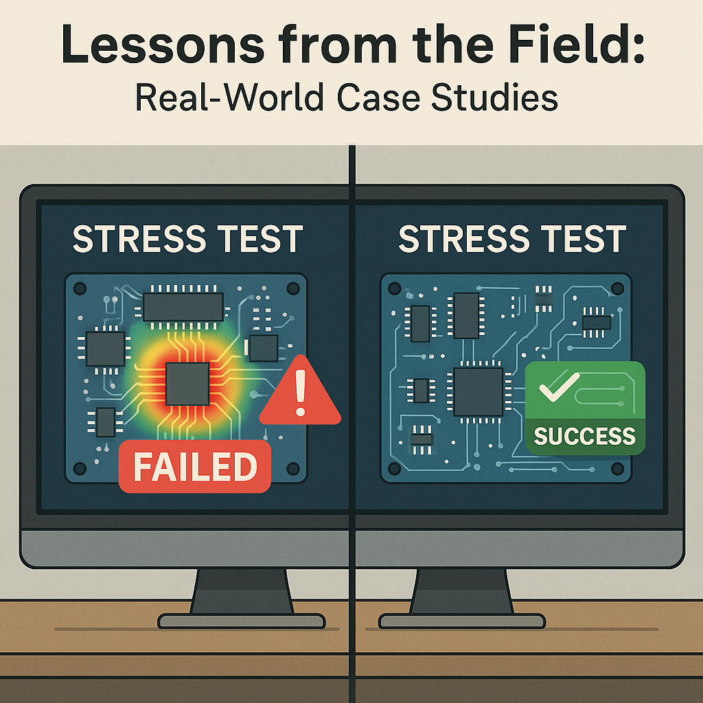
Case Study 2: Mitigating a Thermal Hotspot
A powerful processing component was exceeding its maximum junction temperature during full-load testing. Thermal imaging identified a severe hotspot on the component's surface, indicating inefficient heat removal. The thermal path was clearly inadequate for the power dissipation.
The team implemented a multi-pronged solution. The PCB stack-up was changed to include thicker copper planes, a dense grid of thermal vias was added under the component, and a higher-performance TIM was selected. These changes created an effective thermal path, resolving the issue.
Case Study 3: Tracing a Conformal Coating Defect
A batch of finished assemblies exhibited widespread conformal coating delamination. The defect was not present in previous batches, suggesting a process change or contamination event. The challenge was to find the "needle in a haystack" root cause.
Using the MES traceability data, the team isolated the failure to a specific production day. Further investigation revealed that an unauthorized, silicone-based cleaning agent had been used on the line that day. This contamination was the root cause. Traceability data was key to the quick resolution.
FAQs
Q: What do these case studies show?
A: They show how combining systematic analysis with design and process principles solves real-world problems.